MEE at SMTA International Technical Conference
posted October 2015Three MEE staff members, Larry Hanke, Dieter Scholz and Roberta Rott attended the Surface Mount Technology Association conference this week in Chicago IL. With three of us there it allowed us to always have someone at our booth in the exhibit hall while others could attend technical talks or participate in SMTA committee meetings.
SMTA is a non-profit international association of companies and individuals involved in all aspects of the electronics industry. The constantly evolving electronics industry presents materials problems that require specialized equipment and creative solutions. MEE has long been a leader in laboratory testing applying traditional and advanced analytical methods to help address product challenges efficiently and effectively.
Visit our website to see examples of typical MEE projects for electronic components and a case study on failed printed circuit boards.
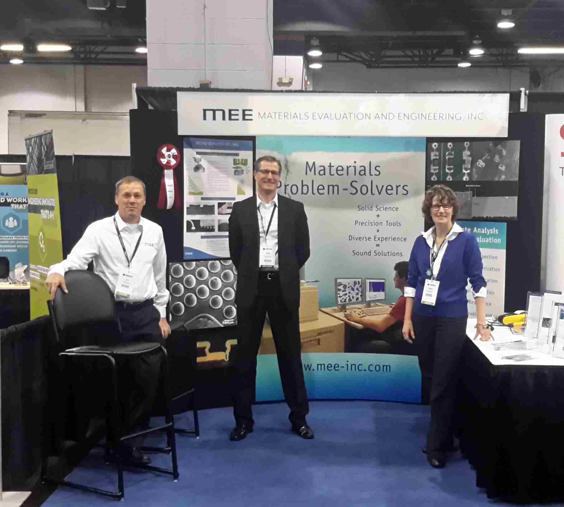
We would like to tell you that the red and white ribbon on our booth indicates a “best of show – trade show booth” but it is there to identify MEE as a corporate sponsor of SMTA.
Filed under: About MEE, Case Studies, integrated circuits, microelectronics, semi-conductor devices,