Category Archives: semi-conductor devices

ASM Board Appointment

posted June 2020

Larry Hanke, P.E. CEO, Materials Evaluation and Engineering, Inc


MEE’s CEO/Senior Engineer, Larry Hanke, was just appointed to the Board of the ASM International Metallographic Society (IMS).

The Metallographic Society is a professional organization serving those involved in the examination, analysis, characterization, structure and evaluation of materials.  Service on the IMS Board of Directors involves planning and driving the future strategy of the society.

Congratulations Larry!

Three MEE staff members, Larry Hanke, Dieter Scholz and Roberta Rott attended the Surface Mount Technology Association conference this week in Chicago IL. With three of us there it allowed us to always have someone at our booth in the exhibit hall while others could attend technical talks or participate in SMTA committee meetings.

SMTA is a non-profit international association of companies and individuals involved in all aspects of the electronics industry. The constantly evolving electronics industry presents materials problems that require specialized equipment and creative solutions. MEE has long been a leader in laboratory testing applying traditional and advanced analytical methods to help address product challenges efficiently and effectively.

Visit our website to see examples of typical MEE  projects for electronic components and a case study on failed printed circuit boards.

Booth STMA Chicago 2015_cropped

We would like to tell you that the red and white ribbon on our booth indicates a “best of show – trade show booth” but it is there to identify MEE as a corporate sponsor of SMTA.

Last week, Larry Hanke presented a paper co-authored with Dieter Scholz at the 2015 Microscopy Society of America (MSA) annual meeting in Portland, Oregon. The presentation, Microstructure Enhancement Using Ion Beam Milling, was based on work done in our laboratory preparing challenging samples for microscopic evaluation.

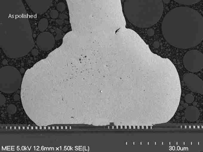
These images show a gold ball bond on an integrated circuit. In the top image we see the sample after it was mechanically prepared/polished. The next image was taken after the sample was ion milled.

- As polished

– As polished

 - Ion Milled

– Ion Milled

Microscopic inspection for device quality assurance, failure analysis, and materials characterization relies on optimum sample preparation to produce accurate and useful data. Good sample preparation for medical devices, semiconductors, microelectronics, and nano-materials has become more challenging in recent years due to high-technology materials, complex assemblies, and smaller components. Although mechanical cross sectioning, polishing, and chemical etching are sufficient for many applications, ion beam milling provides an additional level of quality and clarity for critical and difficult-to-prepare samples.

Broad-Beam Ion Milling

posted June 2015

Senior Scientist, Dieter Scholz, spent a day at the SMTA (Surface Mount Technology Association) 2015 Midwest Expo talking with attendees about the advantages of the Broad-Beam Ion Milling. Ion Beam Milling provides an additional level of quality and clarity for critical and difficult-to-prepare samples. It is particularly useful for cross sections of semi-conductor devices, sectioning of soft materials or soft-hard material combinations or materials difficult to chemically etch.

Dieter and Larry Hanke will be presenting a paper,  Microstructure Enhancement Using Ion Beam Milling, at the Microscopy and Microanalysis 2015 Meeting in Portland OR in August.

Contact us or visit our website for more information on Broad-Beam Ion Milling.


ion mill booth