Category Archives: microscopy

Keyence Digital Light Microscope

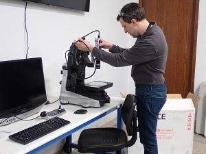
Senior Engineer, Dan Grice is seen here completing the installation of the newest microscope in our inspection lab, a Keyence 7000 series digital light microscope. This is the world’s first 4K ultra-high accuracy microscope. Compared to our current model the expanded features of the 7000 series include 20x greater depth of field, measurement tools allowing measurements directly on screen, 3D display to observe surface contours, adaptive lighting and multi-angle observation. The increased speed and resolution of this microscope will be especially beneficial when we facilitate large joint inspections in our lab.


Microscopy Spring Symposium

posted May 2019

MEE staff to attend Microscopy Spring Symposium

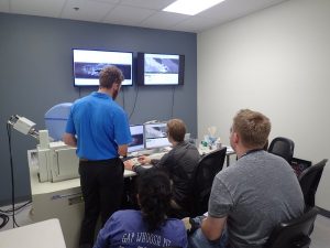
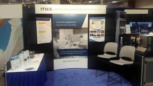
Dieter Scholz and Jason Larson will be attending the Minnesota Microscopy Society’s Annual Spring Symposium on Friday May 3 in St Paul. The topic of this year’s symposium is Non-Traditional and Emerging Microscopy Techniques. MEE is a corporate sponsor of the  MN Microscopy Society and will have a booth at this event. Stop by and say hello to Dieter and Jason and ask about MEE’s expanded laboratory facilities and the new microscopes we have acquired, including the new JEOL IT500HR Scanning Electron Microscope.

Dieter Scholz

Jason Larson

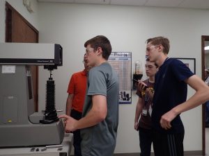
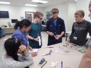
Last Thursday we hosted thirty high school students at MEE  as part of a week-long Materials Science Camp sponsored by the MN Chapter of ASM International.  Under the direction of  industry and academic based “Materials Mentors”, students learned about the process of running a failure analysis investigation. MEE provided a space for the students to get hands on experience with sample preparation, Rockwell hardness testing, light microscopy and scanning electron microscopy.


Three of our staff, Larry Hanke, Kurt Schenk and Neal Hanke, were  camp mentors. This was MEE’s twelfth year sponsoring the camp.

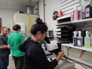
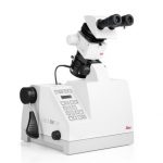
To allow more consistent metallographic section preparation of very small targets, MEE has added a Leica EM/TXP to our selection of sectioning tools. The Leica EM/TXP is specifically designed for more precise and efficient targeting of points of interest in very small specimens. A combination mill/grinder/polisher and stereomicroscope, the Leica EM/TXP, allows the technician to observe the sample during preparation improving accuracy in locating microscopic targets.

We weren’t familiar with the Minneapolis city flag until just recently, but were pleasantly surprised to see one of the symbols on it is a microscope. That seems fitting to us! Microscopes are one of the most important tools we use at MEE to provide our clients in the medical device, industrial and electronics industries with high-quality materials characterization for their advanced materials and critical components.

MEE has three scanning electron microscopes (and a new one coming this summer) and a light microscopy laboratory equipped with a variety of light microscopes with magnifications ranging from 5X to 2,400X.

There is a small contingent of Minneapolis citizens advocating for an update of the flag. We would hate to see the microscope image go away but either way, MEE will always be flying the microscopy banner.


City of Minneapolis Flag

Nanostructures Imaging

posted January 2018

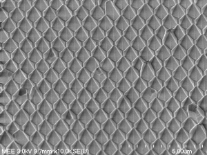
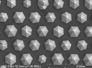
These images are of a selective area of AlGaN (aluminum gallium nitride) nanostructures on graphene. Images were captured using the Field Emission Scanning Electron Microscope, FESEM, at MEE in support of a project partnership between CrayoNano AS of Norway and Agnitron Technology of Eden Prairie, MN USA.

AlGaN Nanostructure

AlGaN Nanostructure

AlGaN Nanostructure

The FESEM is an advanced microscope offering increased magnification and the ability to observe very fine features at a lower voltage than the SEM found in most laboratories.  Just as important as having the right tools for the job is having an experienced operator who can use the microscope to reveal the best images. Kudos to Kurt Schenk, MEE Laboratory Manager, for his work on this fascinating project.

MMS Spring Symposium

posted April 2016

MEE staff members, Larry Hanke, Kurt Schenk and Dieter Scholz will be attending the Minnesota Microscopy Society Spring Symposium on April 29 at the Science Museum in St Paul. Speakers this year will be presenting on failure analysis in plastics, medical devices and water systems.

MEE will be sponsoring a booth in the exhibition hall. Be sure to stop by and say hello.


Filed under: About MEE, microscopy,

Let it Snow!

posted December 2015

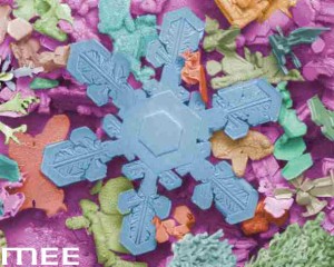
Fun image from our files. This image was created by capturing snow and frost on a chilled aluminum block. The sample was then digitally imaged using the scanning electron microscope. Color was added to the black and white image using graphic editing software.SNOW 8x10 logo dg


MD&M 2015

posted November 2015

It was a fun couple of days in the Exhibit hall of MD&M. Thanks to all who stopped by to talk with us.

MD&D2015-1

Newest design of our booth features the JEOL JSM-6610 LV scanning electron microscope.

We enjoyed the opportunity to talk about our laboratory and engineering services for those in the medical device industry. Almost everyone on staff had a chance to spend some time at the MEE booth and also some time strolling around the exhibit hall to see what was new.  This was MEE’s 16th year with a booth at MD&M.


Last week, Larry Hanke presented a paper co-authored with Dieter Scholz at the 2015 Microscopy Society of America (MSA) annual meeting in Portland, Oregon. The presentation, Microstructure Enhancement Using Ion Beam Milling, was based on work done in our laboratory preparing challenging samples for microscopic evaluation.

These images show a gold ball bond on an integrated circuit. In the top image we see the sample after it was mechanically prepared/polished. The next image was taken after the sample was ion milled.

- As polished

– As polished

 - Ion Milled

– Ion Milled

Microscopic inspection for device quality assurance, failure analysis, and materials characterization relies on optimum sample preparation to produce accurate and useful data. Good sample preparation for medical devices, semiconductors, microelectronics, and nano-materials has become more challenging in recent years due to high-technology materials, complex assemblies, and smaller components. Although mechanical cross sectioning, polishing, and chemical etching are sufficient for many applications, ion beam milling provides an additional level of quality and clarity for critical and difficult-to-prepare samples.