Auger Electron Spectroscopy (AES) provides information about the chemical composition of the outermost material comprising a solid surface or interface. The principal advantages of AES over other surface analysis methods are excellent spatial resolution (< 1 µm), surface sensitivity (~20 Å), and detection of light elements. Detection limits for most elements range from about 0.01 to 0.1% (atomic).
AES uses a primary electron beam to excite the sample surface. When an inner-shell electron is ejected from a sample atom by the interaction with a primary electron, an electron from an outer shell fills the vacancy. To compensate for the energy change from this transition, an Auger electron or an x-ray is emitted. For light elements, the probability is greatest for the emission of an Auger electron, which accounts for the light-element sensitivity for this technique.
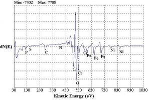
The energy of the emitted Auger electron is characteristic of the element from which it was emitted. Detection and energy analysis of the emitted Auger electrons produces a spectrum of Auger electron energy versus the relative abundance of electrons. Peaks in the spectrum identify the elemental composition of the sample surface. In some cases, the chemical state of the surface atoms can also be determined from energy shifts and peak shapes.
Auger electrons have relatively low kinetic energy, which limits their escape depth. Any Auger electrons emitted from an interaction below the surface will lose energy through additional scattering reactions along its path to the surface. Auger electrons emitted at a depth greater than about 2 – 3 nm will not have sufficient energy to escape the surface and reach the detector. Thus, the analysis volume for AES extends only to a depth of about 2 nm. Analysis depth is not affected by the energy of the primary electron energy.
The AES instrumentation can include a tungsten filament or field emission electron gun for the primary electron beam. The instruments are equipped for secondary electron imaging (SEM) to facilitate location of selected analysis areas, and micrographs of the sample surface can be obtained. The sample chamber is maintained at ultrahigh vacuum to minimize interception of the Auger electrons by gas molecules between the sample and the detector. Some instruments include special stages for fracturing samples to examine interfaces that have been freshly exposed within the vacuum chamber. A computer is used for acquisition, analysis, and display of the AES data.
Survey Scan – The position of the peaks in the AES spectrum obtained in a survey scan identifies the elemental composition of the uppermost 20 Å of the analyzed surface.
Multiplex Scan – A higher resolution analysis of the Auger spectrum in the region around a characteristic peak is used for determination of the atomic concentration of the elements identified in the survey scans and, in some cases, chemical state information.
Quantitation – The AES analysis results can be quantified without standards by using the area under the peaks in the AES spectrum and corrections based on elemental sensitivity factors.
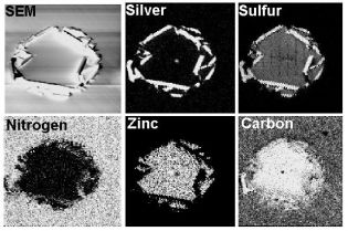
Mapping and Line Scans – These are imaging techniques that measure the lateral distribution of elements on the surface. The electron beam is scanned across the sample surface, either along a fixed line (line scan) or across a given area (mapping) while the AES signal is analyzed for specific energy channels. The AES signal intensity is a function of the relative concentration of the element(s) corresponding to the selected energy channel(s). Spatial resolution is approximately 0.3 µm.
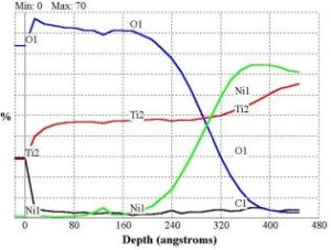
Depth Profile – Material is removed from the surface by sputtering with an energetic ion beam concurrent with successive AES analyses. This process measures the elemental distribution as a function of depth into the sample. Depth resolution of < 100 Å is possible.
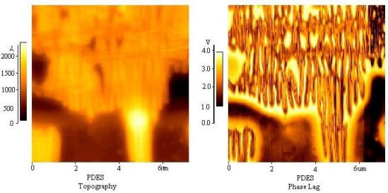
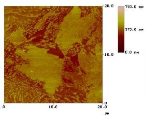
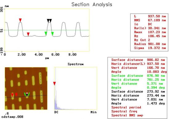
Image Analysis– Since the images are collected in digital format, a wide variety of image manipulations are available for AFM data. Quantitative topographical information, such as lateral spacing, step height, and surface roughness are readily obtained. Images can be presented as two-dimensional or three-dimensional representations in hard copy or as digital image files for electronic transfer and publication.
Nanoindentation – A specialized probe tip is forced into the sample surface to obtain a measure of the material’s mechanical properties in regions as small as a few nanometers. (See the Handbook section on Nanoindentation Hardness Testing.)
- Microscopic particle identification
- Passive oxide film thickness
- Contamination on integrated circuits
- Quantitation of light element surface films
- Mapping spatial distribution of surface constituents