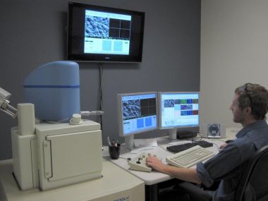
Scanning electron microscopy (SEM) is a method for high-resolution imaging of surfaces. The SEM uses electrons for imaging, much as a light microscope uses visible light. The advantages of SEM over light microscopy include much higher magnification (>100,000X) and greater depth of field up to 100 times that of light microscopy. Qualitative and quantitative chemical analysis information is also obtained using an energy dispersive x-ray spectrometer (EDS) with the SEM. (See Handbook section on EDS analysis.)
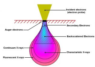
The SEM generates a beam of incident electrons in an electron column above the sample chamber. The electrons are produced by a thermal emission source, such as a heated tungsten filament, or by a field emission cathode. The energy of the incident electrons can be as low as 100 eV or as high as 30 keV depending on the evaluation objectives. The electrons are focused into a small beam by a series ofelectromagnetic lenses in the SEM column. Scanning coils near the end of the column direct and position the focused beam onto the sample surface. The electron beam is scanned in a raster pattern over the surface for imaging. The beam can also be focused at a single point or scanned along a line for x-ray analysis. The beam can be focused to a final probe diameter as small as about 10 Å.
To create an SEM image, the incident electron beam is scanned in a raster pattern across the sample’s surface. The emitted electrons are detected for each position in the scanned area by an electron detector. The intensity of the emitted electron signal is displayed as brightness on a display monitor and/or in a digital image file. By sychromizing the position in the image scan to that of the scan of the incident electron beam, the display represents the morphology of the sample surface area. Magnification of the image is the ratio of the image display size to the sample area scanned by the electron beam.The incident electrons cause electrons to be emitted from the sample due to elastic and inelastic scattering events within the sample’s surface and near-surface material. High-energy electrons that are ejected by an elastic collision of an incident electron, typically with a sample atom’s nucleus, are referred to as backscattered electrons. The energy of backscattered electrons will be comparable to that of the incident electrons. Emitted lower-energy electrons resulting from inelastic scattering are called secondary electrons. Secondary electrons can be formed by collisions with the nucleus where substantial energy loss occurs or by the ejection of loosely bound electrons from the sample atoms. The energy of secondary electrons is typically 50 eV or less.
Two electron detector types are predominantly used for SEM imaging. Scintillator type detectors (Everhart-Thornley) are used for secondary electron imaging. This detector is charged with a positive voltage to attract electrons to the detector for improved signal to noise ratio. Detectors for backscattered electrons can be scintillator types or a solid-state detector.
The SEM column and sample chamber are at a moderate vacuum to allow the electrons to travel freely from the electron beam source to the sample and then to the detectors. High-resolution imaging is done with the chamber at higher vacuum, typically from 10-5 to 10-7 Torr. Imaging of nonconductive, volatile, and vacuum-sensitive samples can be performed at higher pressures.
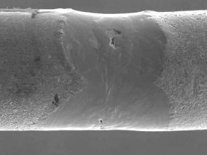
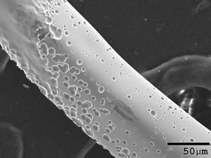
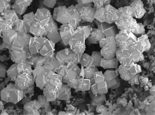
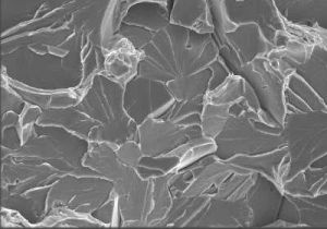
Secondary Electron Imaging – This mode provides high-resolution imaging of fine surface morphology. Inelastic electron scattering caused by the interaction between the sample’s electrons and the incident electrons results in the emission of low-energy electrons from near the sample’s surface. The topography of surface features influences the number of electrons that reach the secondary electron detector from any point on the scanned surface. This local variation in electron intensity creates the image contrast that reveals the surface morphology. The secondary electron image resolution for an ideal sample is about 3.5 nm for a tungsten-filament electron source SEM or 1.5 nm for field emission SEM.
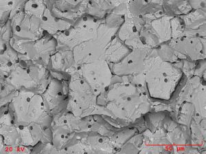
Backscatter Electron Imaging – This mode provides image contrast as a function of elemental composition, as well as, surface topography. Backscattered electrons are produced by the elastic interactions between the sample and the incident electron beam. These high-energy electrons can escape from much deeper than secondary electrons, so surface topography is not as accurately resolved as for secondary electron imaging. The production effeciency for backscattered electrons is proportional to the sample material’s mean atomic number, which results in image contrast as a function of composition, i.e., higher atomic number material appears brighter than low atomic number material in a backscattered electron image. The optimum resolution for backscattered electron imaging is about 5.5 nm.
Variable Pressure SEM – Traditionally, SEM has required an electrically-conductive sample or continuous conductive surface film to allow incident electrons to be conducted away from the sample surface to ground. If electrons accumulate on a nonconductive surface, the charge buildup causes a divergence of the electron beam and degrades the SEM image. In variable-pressure SEM, some air is allowed into the sample chamber, and the interaction between the electron beam and the air molecules creates a cloud of positive ions around the electron beam. These ions will neutralize the negative charge from electrons collecting on the surface of a nonconductive material. SEM imaging can be performed on a nonconductive sample when the chamber pressure is maintained at a level where most of the electrons reach the sample surface, but there are enough gas molecules to ionize and neutralize charging. Variable pressure SEM is also valuable for examination of samples that are not compatible with high vacuum.
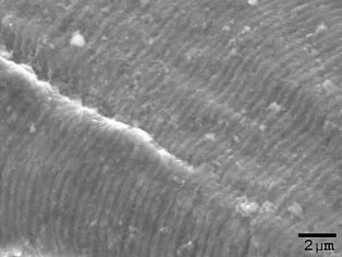
Field Emission SEM (FESEM) – SEMs that use a thermal emission source (i.e., tungsten filament) to generate the electron beam are generally adequate for most samples and provide satisfactory resolution at magnifications up to about 100,000X. However, for high resolution and high magnification imaging a cold field emission (FE) gun provides the best resolution available for SEM. The cold FE gun extracts electrons from the FE cathode by applying a strong electrical field close to a very sharp tip. This method of electron extraction results in a higher electron yield and a smaller beam size, which thus provides a brighter signal with better resolution.
The useful magnification for FESEM imaging ranges up to 500,000X. A second advantage of FESEM is that high resolution imaging can be performed with very low accelerating voltages. At low voltage, very fine features are more readily observed and many non-conductive materials can be examined without applying a conductive coating. Low voltage FESEM examination is ideal for imaging nano-materials, polymers, and thin films.
Quantitation – Image magnification is calibrated against a reference standard. Lateral feature dimensions can be readily quantified to an accuracy of less than 0.1 µm. Computer analysis of images can quantify area or volume fractions and particle shapes and sizes.
In a large-chamber SEM, samples up to 8 in. (200 mm) in diameter can be readily accommodated. Larger samples, up to 12 in. (300 mm) across can be loaded with limited stage movement. Sample height is typically limited to ~2 in. (50 mm). Backscattered electron imaging can be performed on conductive or nonconductive samples. For secondary electron imaging, samples must be electrically conductive. Nonconductive materials can be evaporatively coated with a thin film of carbon, gold or other conductive material to obtain conductivity without significantly affecting observed surface morphology.
Samples must be compatible with at least a moderate vacuum. For high-resolution secondary electron imaging, the sample environment is at a pressure of 1 x 10⁻⁵ Torr or less. The pressure can be adjusted up to about 2 Torr for vacuum sensitive samples.