Cracking Capacitors
Several printed circuit board (PCBs), each with 5 multilayer ceramic capacitors (MLCCs), were evaluated to characterize the capacitors. Each PCB was about 1 in. by 1 in. square. Four of the MLCCs were parallel to one edge of the PCB, and one MLCC was oriented at 90° to the others. Some of the capacitors had failed in testing and were suspected to be cracked. The MLCCs were inspected by scanning electron microscopy (SEM) as received. All the MLCCs were metallographically sectioned, the prepared cross sections were examined by light microscopy.
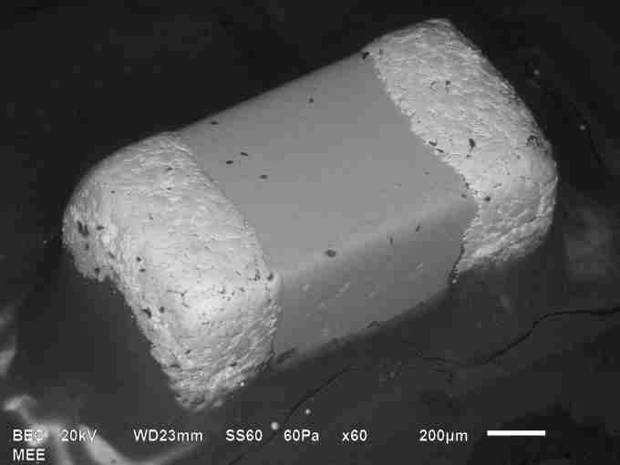
No cracks nor other anomalies were observed by the as-received SEM inspection. However, metallographic sectioning and light microscopy revealed cracks at the bottom corners of several capacitors. The cracks ran from the edge of the termination toward the end face of the MLCC. The cracks were not visible by SEM of the as-received samples because the cracks were contained within the MLCC ceramic and did not extend through the end metal termination and solder. Additionally, the cracks extended toward the PCB and thus would not be visible without removing the capacitors from the PCB.
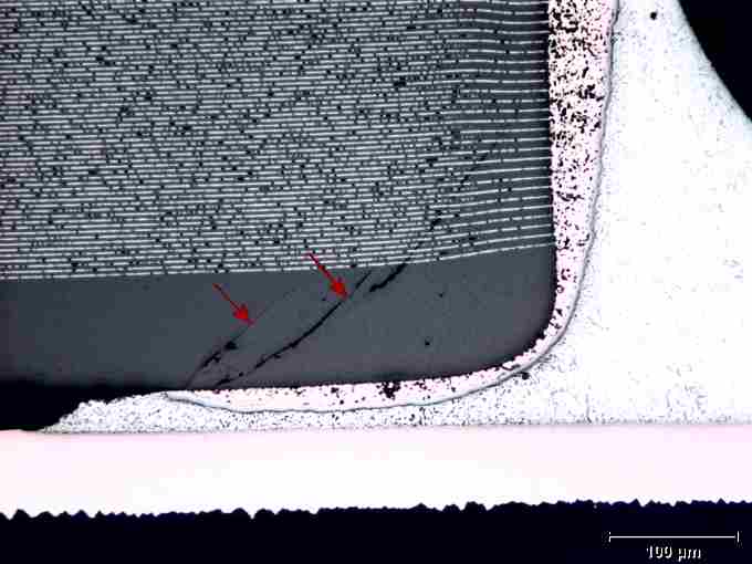
Cracks were observed only for the 4 capacitors that were parallel to each other. No cracks were observed for the one capacitor that was oriented perpendicular to the others. The shape and morphology of the cracks were characteristic of cracks created as a result of PCB bending.
Further investigation revealed that the PCBs were processed as part of a larger PCB panel consisting of an array of 8 individual PCBs. The small PCBs were depanelled after all the devices were soldered to the PCB. The larger PCB panel was about 8 in. long and 1 in. wide, i.e, a single row of 8 smaller PCBs. All of the MLCCs with cracks were parallel to the original 8-in. length of the panel, whereas the MLCCs perpendicular to the 8-in. length were all intact. Thus, the cracking of the MLCCs was due to flexing along the length of the PCB panel prior to or during depanelling into the 1 in. square final product. The MLCCs that were perpendicular to the 8-in. length were subjected to much less stress than those parallel to the length when the panel was flexed, so these capacitors did not crack. Revision of the PCB layout so that all MLCCs would be soldered perpendicular to the length of the original PCB panel was recommended. Less stressful processing, such as laser depaneling, could also prevent future failures.
Ceramics are inherently brittle materials that may crack during metallographic sample preparation if not handled properly. For this evaluation, the combination of the brittle ceramic, the soft solder, the copper traces, and the fiberglass PCB substrate creates a real challenge to prepare a cross section specimen such that all the materials are well preserved and polished. MEE has the expertise to prepare difficult samples, so clients can have confidence in the results. The evaluation presented in this case study included metallography, light microscopy, and scanning electron microscopy (SEM). For specific details on these methods, please see the Handbook of Analytical Methods of Materials on our website or contact us for more information.